We have seen in Figure 10-20 that etching (i.e., the dissolution or physical or chemical removal of material) is also an important step in the fabrication process. Etching takes on a priority role in microelectronics manufacturing because of the need to create well-defined structures from an essentially homogeneous material. In integrated circuits, etching is necessary to remove unwanted material that could provide alternative pathways for electrons and thus hinder operation of the circuit. Etching is also of vital importance in the fabrication of micromechanical and optoelectronic devices. By selectively etching semiconductor surfaces, it is possible to fabricate motors and valves, ultrasmall diaphragms that can sense differences in pressure, or cantilever beams that can sense acceleration. In each of these applications proper etching is crucial to remove material that would either short out a circuit or hinder movement of the micromechanical device.
A. Dry Etching
Dry etching involves gas-phase reactions (usually in plasmas) that form highly reactive species that impinge on the surface to react with the surface, to erode the surface, or both. In the fabrication of optoelectronic devices, dry etching is used almost exclusively. Indium phosphide (InP) is a material that is used in the fabrication of optoelectronic devices, but it is an extremely difficult material to etch.
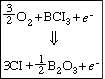
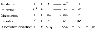
One technique that has been used to etch InP successfully is reactive ion etching (RIE). RIE involves the formation of highly reactive species, usually in a plasma, that impinge on the surface to react with and to erode the surface. To illustrate the principles of RIE, we will study the etching of InP in an argon plasma. Typical reactions that occur in the gas-phase plasma (which generates high-energy electrons) are
A schematic of the plasma is shown in Figure R10.3-1.
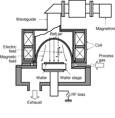
Figure R10.3-1
Schematic of ion bombardment taking place on the wafer
(Courtesy of Semiconductor Int., 15 (6) 72 (1992)
Typical operating conditions are shown in Table R10.3-1.
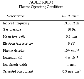
Figure R10.3-2 shows a schematic of the various processes occurring in the plasma directly above the surface to be etched as well as those occurring in the substrate. 3 As shown in Figure R10.3-2, the incident ion may either be reflected and neutralized, causing the surface to eject an electron or atom (sputtering) or be implanted in the surface. Any or all of these processes can result in structural rearrangement of the surface, making the surface move reactive to other gas molecules (e.g., Cl) present in the plasma.
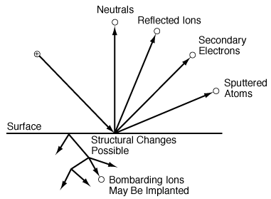
Figure R10.3-2
Plasma interactions with a surface
We now look specifically at the reactive ion etching of InP. The removal of InP from the surface can occur by two mechanisms. In the first mechanism, InP is removed as a result of bombardment from a high-energy argon ion that knocks InP off the surface. This type of etch, called sputtering or sputter etching, is simply erosion of the surface; no chemical reactions are involved (Figure R10.3-3). In the second mechanism a reaction takes place between InP and chlorine to form InCl.
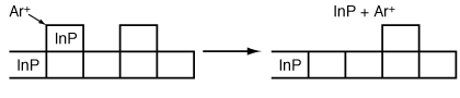
Figure R10.3-3
Etching by sputtering
The more volatile InCl 3 is removed from the surface either by argon or by vaporization ion bombardment (Figure R10.3-4). Because a reaction takes place before removal of the material it is called reactive ion etching. We shall now consider the RIE of InP in more detail.
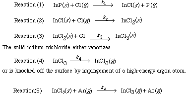
The chlorine atoms that are generated react with the surface according to the following sequence: 4
This last step is a sputtering reaction.
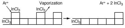
Figure R10.3-4
RIE etching
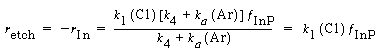
We now proceed to prepare a law for the rate of etching in terms of the concentrations of argon and chlorine. We assume that each step in the etching process is elementary. The net rate of removal of indium from the surface is the sum of that removed by both Reactions (4) and (5):

(R10.3-1)
where (Ar) is the concentration of argon above the surface and is the fraction of the surface covered by InCl 3.
Net Rate of Formation of Reactive Intermediates. The chemical species InCl and InCl 2 are unstable reactive intermediates. Because the etching takes place at steady state, there is no net rate of formation of these species. That is, they react virtually as fast as they are formed. For Reactions (1) and (2), which are elementary, the net rate is
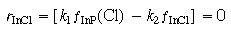
(R10.3-2)
Solving for the fraction of the surface covered by InCl gives
(R10.3-3)
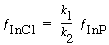
Similarly, the net rate of formation of InCl 2 is zero, and Reactions (2) and (3) give
(R10.3-4)
Solving for the fraction of surface covered by InCl 2 yields
(R10.3-5)
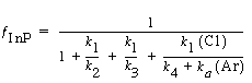
Finally, the net rate of formation of InCl 3 is also zero at steady state. Reactions (3), (4), and (5) give

(R10.3-6)
Solving for the fractional coverage of InCl 3 , we obtain
(R10.3-7)
Next we carry out a fractional surface-area balance:
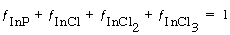
(R10.3-8)
Substituting for InCl, InCl 2 , and InCl 3yields
(R10.3-9)
Combining Equations (R10.3-1) and (R10.3-7), we obtain
(R10.3-10)
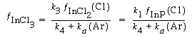
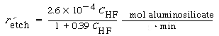
Substituting for°InP in Equation (R10.3-10), and multiplying numerator and denominator by and dividing by k 1 , the etch rate law for RIE of indium phosphide becomes
(R10.3-11)
where
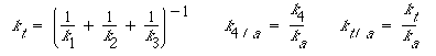
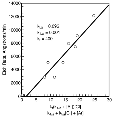
Figure R10.3-5
A nonlinear least squares analysis (discussed in Chapter 5) gives k t = 400, k 4/A = 0.001, and k t/A = 0.095. Figure R10.3-5 shows the experimental etch rate as a function of the predicted etch rate shown on the right-hand side of Equation (R10.3-11). A photo-correlation spectros copy analysis of the surface being etched reveals that the surface is primarily InP and InCl 3 , with virtually no InCl and InCl 2 :
Consequently, for all practical purposes the etch rate can be written as
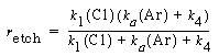
(R10.3-12)
B. Wet Etching
Wet etching is used primarily in micromachining, where acids are used to dissolve the solid substrate to form intricate channels and slopes, but it has also been used in the fabrication of computer chips. Figure R10.3-6 shows a schematic of the etching process of material A. When a chemical etch is to be carried out, the portion of the material that is not to be etched is covered by a polymer coating called a photoresist, which prevents it from contacting the acid.
Next, the area of material A that is unprotected by the photoresist is etched away until the acid reaches material B and completes the channel formation. Finally, the photoresist is removed by immersing the chip in the appropriate solvent. In many instances we want to stop the etching process as soon as we reach the A/B interface. To achieve this etch stop as precisely as possible, we need to know the rate of etching. Consequently, in this section we
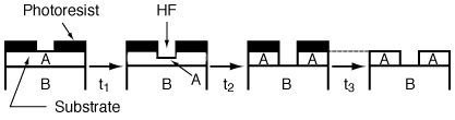
Figure R10.3-6
Wet etching
focus on the rate of etching (i.e., rate of dissolution of solid materials) to develop mechanisms and rate laws.
As an example of etching, consider the dissolution of a silicate in hydrofluoric acid. First consider the dissolution in which no liquid-phase catalysts are used. The acid, A (e.g., HF), adsorbs reversibly on a site S on the substrate surface (Figure R10.3-7). Symbolically, we have
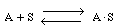
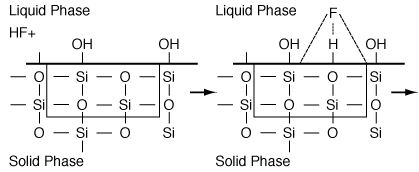
Figure R10.3-7
Adsorption of HF
The adsorbed acid breaks the Si-O bonds on the substrate surface, thereby dissolving it and generating products that go into the liquid phase. These products (Si, O) undergo a series of rapid homogeneous reactions which produce SiF4 and H 2 O. When these products go into solution, they uncover the next molecular layer of substrate to be dissolved, as shown in Figure R10.3-8.
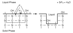
Figure R10.3-8
Surface reaction
We can write the surface reaction symbolically as
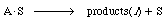
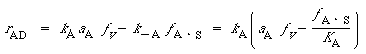
The symbol S in this reaction represents the new substrate surface that has been exposed to acid after the layer above it has been removed. As with catalytic reactions, the surface reaction is most often rate-limiting, in which case we have

(R10.3-13)
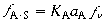
where fA S is the fraction of the surface that has A adsorbed. For the adsorption step, the rate of adsorption
(R10.3-14)
where a A is the activity of the acid in solution. For ideal solutions we can replace a by the concentration C A . Because surface reaction is rate-limiting,
(R10.3-15)
The fractional surface area balance is

(R10.3-16)
Substituting for fAS and solving for f v gives us
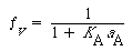
(R10.3-17)
Combing Equations (R10.3-13), (R10.3-15), and (R10.3-17), we obtain the etch rate as
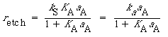
(R10.3-18)
For activity coefficients of approximately unity, the rate expression becomes
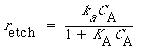
(R10.3-19)
Figure R10.3-9 shows the dissolution of the aluminosilicate montmorillonite as a function of HF concentration. 5 The corresponding rate law is
(R10.3-20)
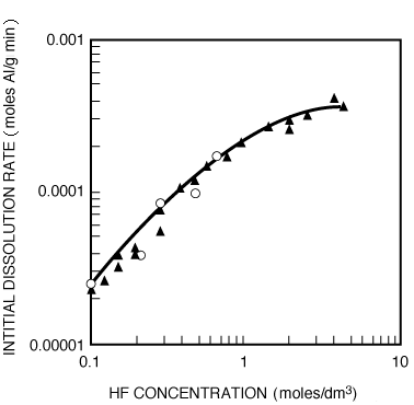
Figure R10.3-9
Rate of etching as a function of HF concentration.